|
|
|
|
|
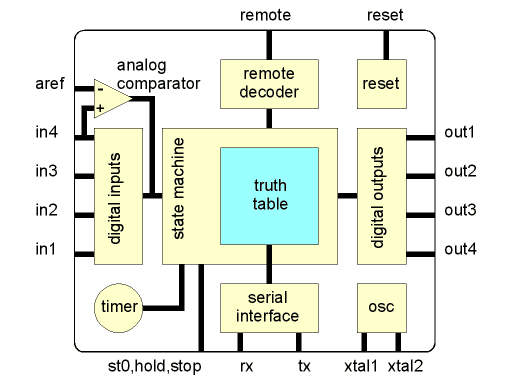
Nutchip input & output
| Block diagram |
|
|
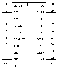
Chip pinout, dual-in-line plastic case.
|
||||||||||||||||||||||||||||||
|
description |
pin # |
|
| /RESET | Chip hardware reset, active low. Must be kept low for 2 clock cycles minimum to ensure proper device reset. | 1 |
| RX, TX | Serial port input (RX) and output (TX) for chip monitoring and programming. | 2, 3 |
| XTAL2 | Clock oscillator (drive pin) | 4 |
| XTAL1 | Clock oscillator sense input / External 4 MHz clock input | 5 |
| REMOTE | Remote control decoder input | 6 |
| /ST0 | State machine reset. Must be kept low for 10 mS minimum to ensure return to state st00. | 7 |
| IN1...IN2 | State machine programmable digital inputs | 8, 9 |
| GND | 0 volts power supply | 10 |
| IN3 | State machine programmable digital input | 11 |
| IN4 (COMP) | State machine programmable digital input/ alternate positive input to the analog comparator (input IN4 = 1 when Vin > Aref) | 12 |
| AREF | Analog voltage reference input | 13 |
| /STOP | State machine stop, active low. | 14 |
| /HOLD | State machine timer hold, active low | 15 |
| OUT1...OUT4 | State machine programmable digital outputs | 16...19 |
| Vcc | +5 volt dc power supply (can range from 4 to 6V) | 20 |
| State machine's truth table memory |
The state machine truth table memory can hold up to(*) 32 different states, 64 input conditions, 6 remote control keys and 30 different timeouts. The truth table memory is loaded through the serial port. No explicit erase is required before writing (auto-erasing).Memory is non-volatile, retains data between power interruptions, and can be rewritten at least 1000 times. Each state includes up to 4 inputs, up to four outputs, and one remote control key.
(*) Maximum capacity, actual capacity varies based on truth table content.