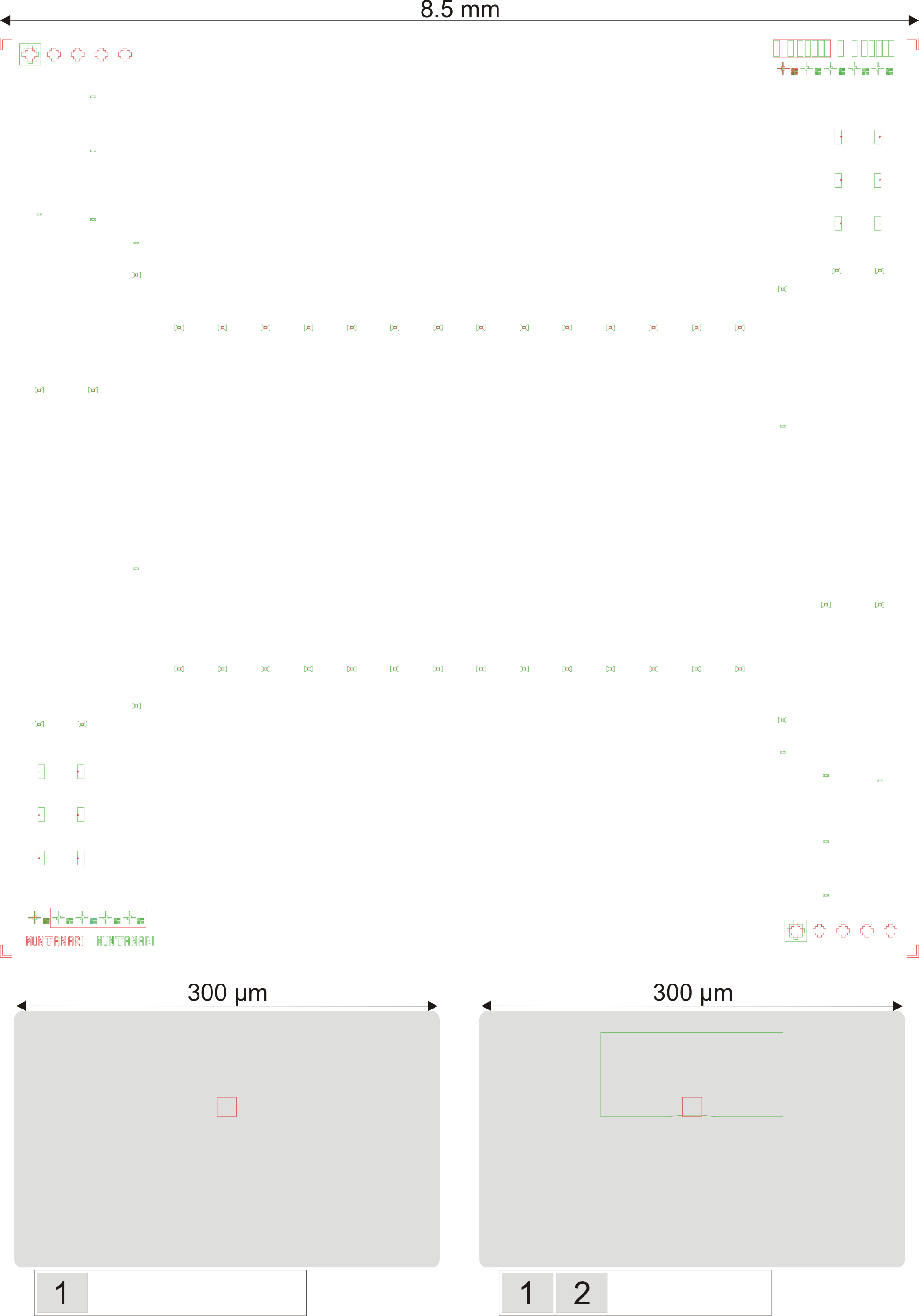
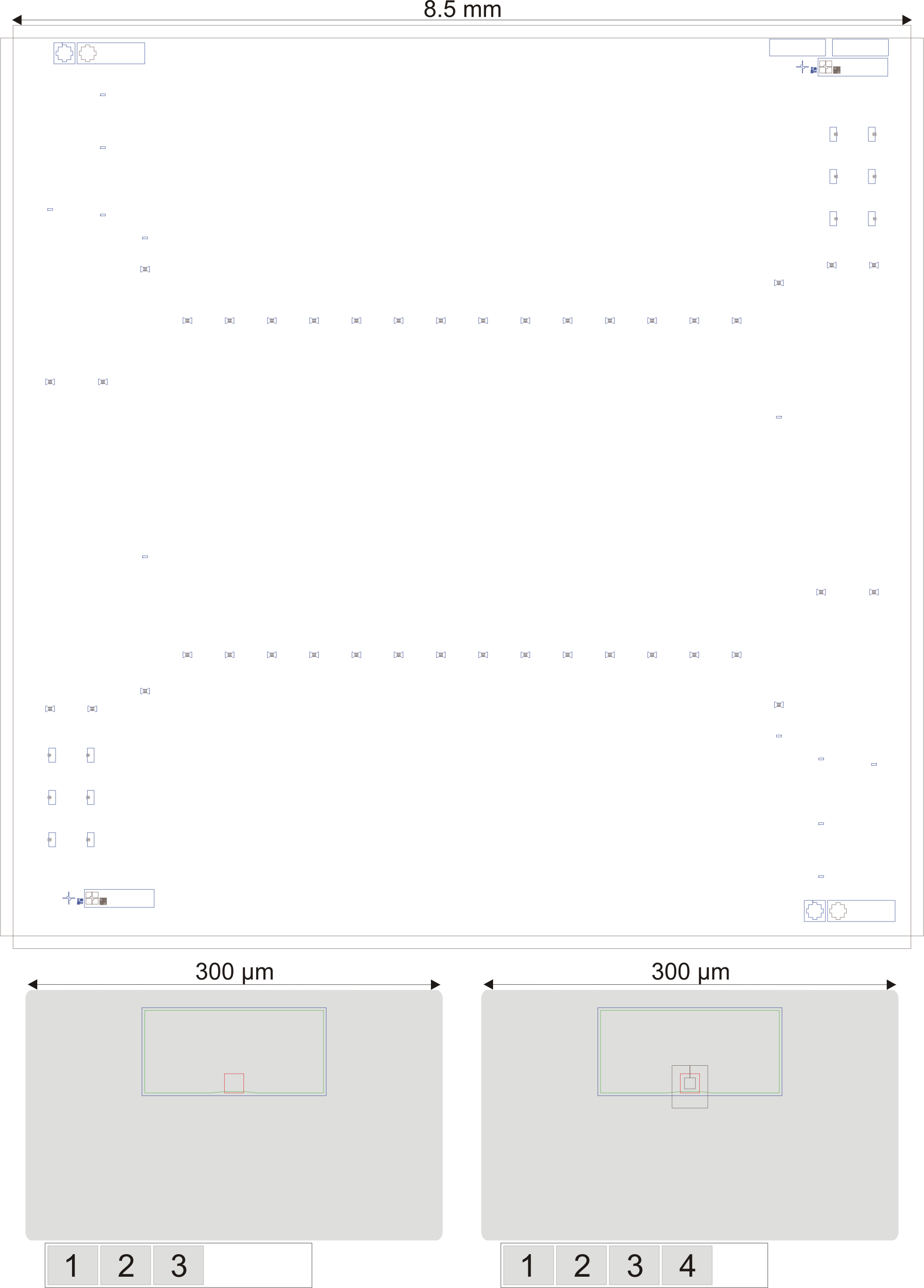
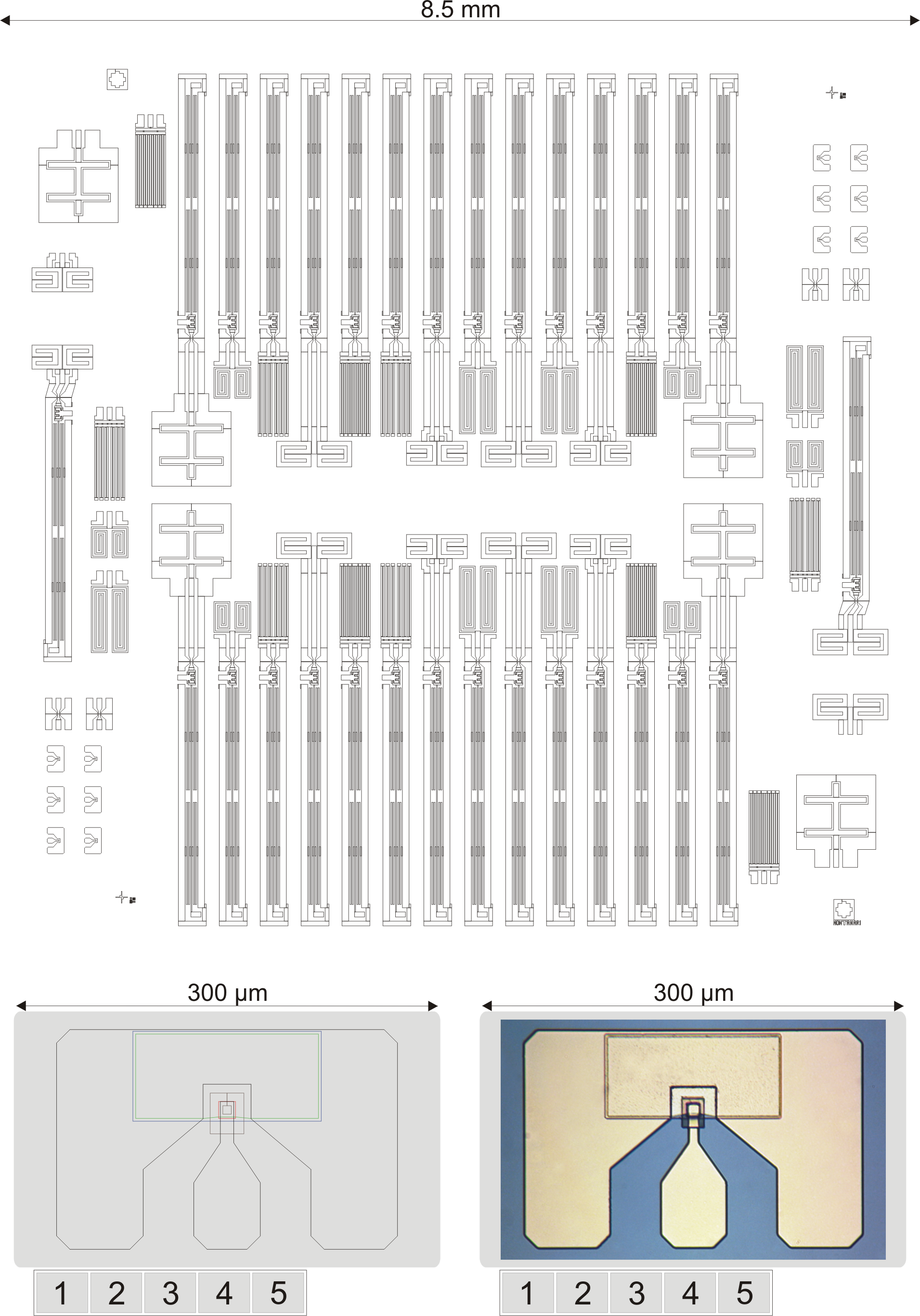
All sets of masks used in this work were designed and fabricated
at IGS-1 in Forschungszentrum Juelich. The optical lithography
mask consists of a glass plate (commonly quartz, borosilicate
glass or fused-silica) on which chromium patterns are defined by
means of electron beam lithography. In this appendix, a brief
overview of the mask layouts is presented focusing on the
polyamide planar process (see section 5). Each step
of the device preparation required an optical lithography mask:
- mesa definition by reactive ion etching;
- self aligned ohmic contacts deposition;
- diode electrical isolation etching;
- diode planarization / passivation;
- bond-pads, low-pass filter and resonant circuit
deposition.
Steps 1, 2 and 5 rely on a positive lithographic process, and
steps 3 and 4 on a negative one.
In the case of the air-bridge process, two further
layers are required. A detailed explanation of the optional
air-bridge process is given in section 5.6.
simone montanari
2005-08-02