Next: 6. Experimental results and Up: Fabrication and characterization of Previous: 4. Experimental Methods Contents
Depending on the compound semiconductor type (GaAs and GaN), each step requires a particular approach. The differences between the adopted solutions for GaAs and GaN will be discussed. A detailed list of the process parameters can be found in appendix C.
For the mesa etching of a Gunn diode, two possibilities are
available: dry Reactive Ion Etching (RIE) and wet chemical
etching. Dry etching has been chosen, because it allows an exact
definition of the mesa5.1, prevents unwanted under-etch and
provides smooth and nearly vertical side-walls. For both GaAs and
GaN mesas, a chlorine based gas mixture is preferable. The demand
of deep mesas requires high etch rates. Chlorine based plasmas are
highly aggressive for Ga-based III-V semiconductor, because the
chloride ![]() is highly volatile [PRA94]. The use of
methan is not indicated for two reasons: the
is highly volatile [PRA94]. The use of
methan is not indicated for two reasons: the ![]() process
presents low etch rates and there is the risk of formation of
solid gallium carbide. The considered etching process ECR
(Electron Cyclotron Resonance) -RIE was proposed by Kaindl at al.
[KSF95] and by Franz et al. [Fra94,FR99]. The ECR-RIE
has been carried out in a Oxford Plasmalab System 90 equipment.
The working principle of ECR is based on the electron cyclotron
frequency:
process
presents low etch rates and there is the risk of formation of
solid gallium carbide. The considered etching process ECR
(Electron Cyclotron Resonance) -RIE was proposed by Kaindl at al.
[KSF95] and by Franz et al. [Fra94,FR99]. The ECR-RIE
has been carried out in a Oxford Plasmalab System 90 equipment.
The working principle of ECR is based on the electron cyclotron
frequency:
In the ECR chamber, the gas mixture is situated between two
magnets, providing a static magnetic field B. In Eq. (5.1)
![]() is the electron charge and
is the electron charge and ![]() is the electron mass. The
plasma is excited by a microwave field in the presence of the
magnetic field of the correct magnitude to cause the electrons to
spiral at the microwave frequency
is the electron mass. The
plasma is excited by a microwave field in the presence of the
magnetic field of the correct magnitude to cause the electrons to
spiral at the microwave frequency ![]() , thus increasing the
probability of ionization. The current flowing in the upper magnet
is
, thus increasing the
probability of ionization. The current flowing in the upper magnet
is
![]() , while the one flowing in the lower magnet
is
, while the one flowing in the lower magnet
is
![]() . The both magnets contribute to realize the
resonance condition; tuning the lower magnet current the
thickness of the ECR layer (accelerating layer) can be changed:
the corresponding the plasma density influences the etch rate and
uniformity [PRA94]. Once the plasma is stable under a
constant pressure of
. The both magnets contribute to realize the
resonance condition; tuning the lower magnet current the
thickness of the ECR layer (accelerating layer) can be changed:
the corresponding the plasma density influences the etch rate and
uniformity [PRA94]. Once the plasma is stable under a
constant pressure of
![]() , the etching process
begins applying a R.F. power of 50-60 W. The RF signal causes a
bias difference between the top and the bottom part of the ECR
chamber and directs the plasma towards the lower part, where the
etching takes place. The main advantage of ECR-RIE is the
separation of the plasma generation region from the one where the
sample is etched. In this way, the sample can be etched smoothly,
reducing the crystal defects induced by the process.
, the etching process
begins applying a R.F. power of 50-60 W. The RF signal causes a
bias difference between the top and the bottom part of the ECR
chamber and directs the plasma towards the lower part, where the
etching takes place. The main advantage of ECR-RIE is the
separation of the plasma generation region from the one where the
sample is etched. In this way, the sample can be etched smoothly,
reducing the crystal defects induced by the process.
The chosen conditions for the GaAs dry etching are listed in
appendix C.4 and are inspired from the optimization
work of Stock [Sto03]. The mesa area is defined evaporating
Ti patterns as etching masks. After the Ti lift-off, an oxygen
plasma treatment removes possible resist traces. Now, it is
possible to start the ECR-RIE with a
![]() gas mixture.
The etch-rate is between 350 and
gas mixture.
The etch-rate is between 350 and
![]() ,
depending on the sample temperature, gas pressure and RF power.
The etch-rate has been monitored sampling the etched thickness
with a Dektak profilometer. The selectivity of the plasma process
between the Ti masks and the GaAs sample is 1:8.
,
depending on the sample temperature, gas pressure and RF power.
The etch-rate has been monitored sampling the etched thickness
with a Dektak profilometer. The selectivity of the plasma process
between the Ti masks and the GaAs sample is 1:8.
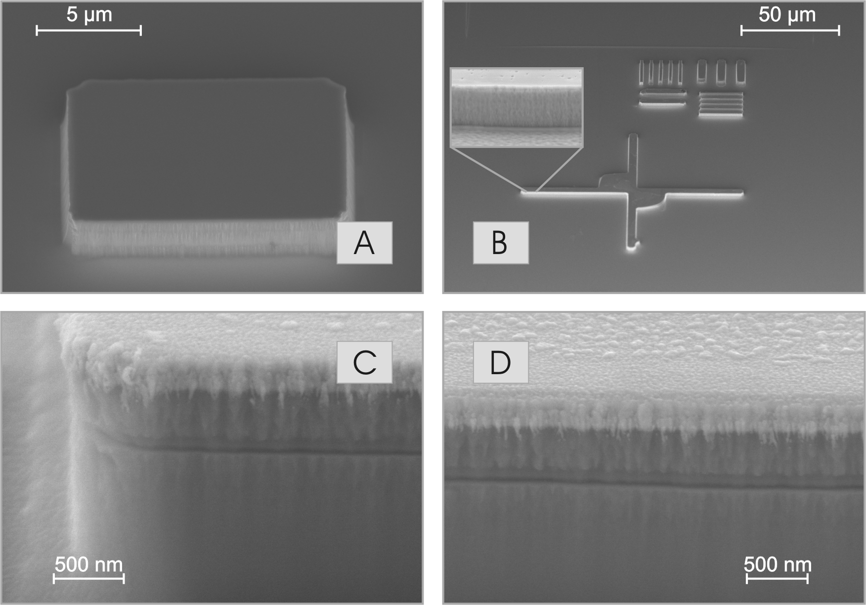
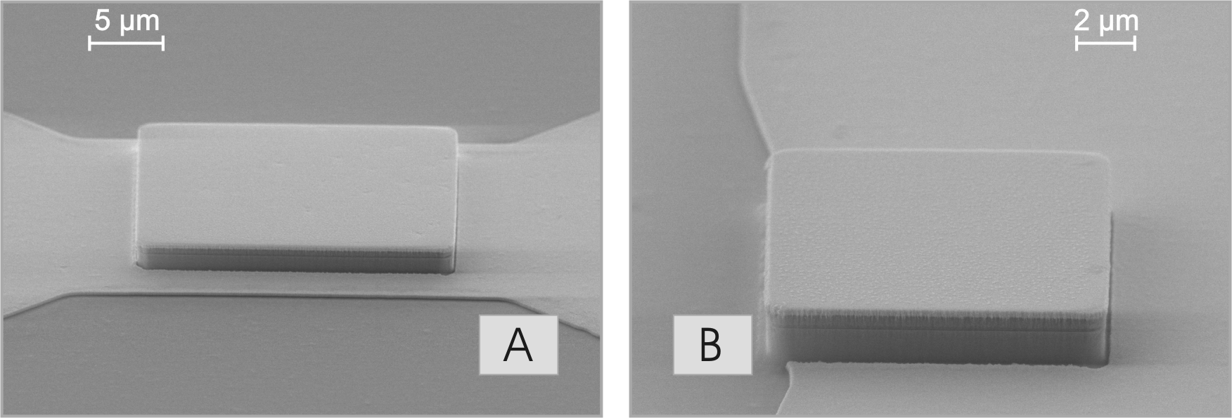
In Fig. 5.1, SEM pictures of the etched GaAs
samples are presented. A typical mesa of a graded gap injector
Gunn diode and an alignment mark pattern are shown in
Fig. 5.1A and B, respectively. The shape of the Ti
mask is perfectly reproduced, no under-etch is present and the
sidewalls are smooth and vertical. After the plasma process, the
Ti mask is easily removed in a hydrofluoric acid (HF) buffered
solution (AF91). HF is not aggressive for GaAs or AlGaAs if the Al
concentration is under 35%. In Fig. 5.1C and D, a
thin horizontal line can be noticed in the sidewalls. The diodes
in pictures C and D, in fact, have a double AlAs thin layer
(resonant tunneling injector). The thin line originates from the
under-etch of the two AlAs layers, during the Ti removal. The
under-etch does not represent a serious threat for the device:
considering a under-etch of about
![]() and a diode
area of about
and a diode
area of about
![]() , the estimated change in
the current is lower than 0.1% .
, the estimated change in
the current is lower than 0.1% .
|
Before the mesa-etching, the ECR-RIE chamber is cleaned, as
described in section 5.1.1. Then, to the GaN
sample, a gas mixture of ![]() is applied. In comparison with
the GaAs process, here hydrogen is not used. For GaAs, hydrogen
plays a moderator role, it reduces the etch-rate and provides
smooth surfaces [vH95]. However, for GaN, the etch-rate is
considerably lower and there is no need of hydrogen. Concerning
the GaN surface morphology, the effect of hydrogen can not be
noticed. Hydrogen is still used to start the plasma, but it is not
present anymore during the etching process.
is applied. In comparison with
the GaAs process, here hydrogen is not used. For GaAs, hydrogen
plays a moderator role, it reduces the etch-rate and provides
smooth surfaces [vH95]. However, for GaN, the etch-rate is
considerably lower and there is no need of hydrogen. Concerning
the GaN surface morphology, the effect of hydrogen can not be
noticed. Hydrogen is still used to start the plasma, but it is not
present anymore during the etching process.
The mask choice for the GaN ECR-RIE was a difficult task. It has
already been shown that using a thin Ti mask and etching with
![]() plasma result in an inhomogeneous etch
profile, with spikes [Jav03]. In our test with
plasma result in an inhomogeneous etch
profile, with spikes [Jav03]. In our test with ![]() gas
mixture, the selectivity between Ti and GaN was low and
significant redeposition next to the mesas has been observed.
Resist and
gas
mixture, the selectivity between Ti and GaN was low and
significant redeposition next to the mesas has been observed.
Resist and ![]() masks have been tried without much success.
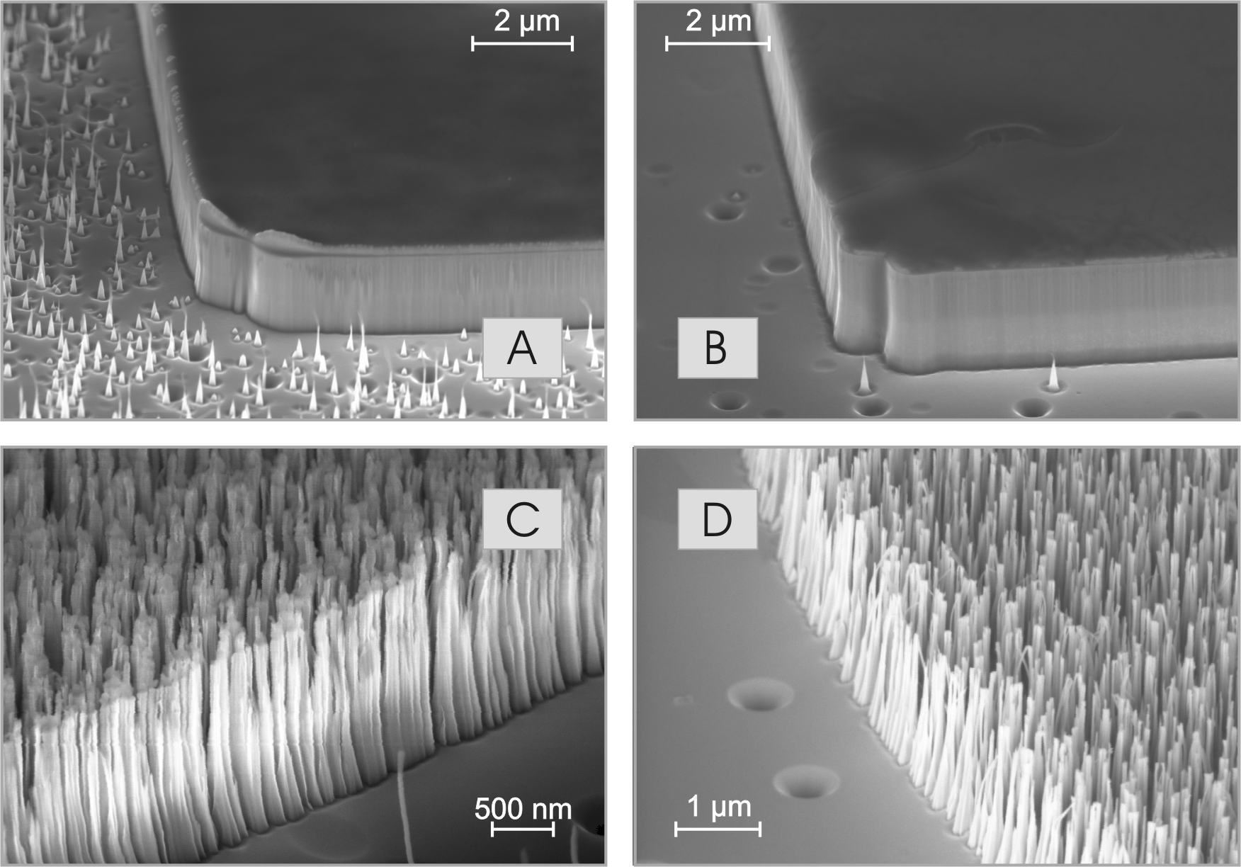
Good results appeared, only, with a mask of evaporated nickel.
Figure 5.2A shows an etched GaN mesa
before the Ni removal. The walls are perfectly vertical and
smooth. The morphology of the etched surface is not regular: GaN
spikes cover the whole etched surface. Figure
5.2B presents a better morphology obtained
after tuning the etch-process: the chamber pressure has been
decreased and the proportions between argon and chlorine have
been modified. The remaining spikes can be eliminated by argon
sputtering.
masks have been tried without much success.
Good results appeared, only, with a mask of evaporated nickel.
Figure 5.2A shows an etched GaN mesa
before the Ni removal. The walls are perfectly vertical and
smooth. The morphology of the etched surface is not regular: GaN
spikes cover the whole etched surface. Figure
5.2B presents a better morphology obtained
after tuning the etch-process: the chamber pressure has been
decreased and the proportions between argon and chlorine have
been modified. The remaining spikes can be eliminated by argon
sputtering.
|
Figure 5.2C and D illustrate GaN
nanocolumns fabricated by ECR-RIE etching. The nanocolumns have
diameters from 30 to 80 nm and heights from 1.4 to 2 ![]() . The
etching is clearly anisotropic and the sidewalls are notably
smooth. The nanocolumns are homogenously distributed on the sample
with a density of
. The
etching is clearly anisotropic and the sidewalls are notably
smooth. The nanocolumns are homogenously distributed on the sample
with a density of
![]() cm
cm![]() and reproduce the Ti
patterns deposited before etching. If we compare the column
density with the estimated dislocation density of the original GaN
wafer (
and reproduce the Ti
patterns deposited before etching. If we compare the column
density with the estimated dislocation density of the original GaN
wafer (![]() cm
cm![]() ), no correlation can be found. In
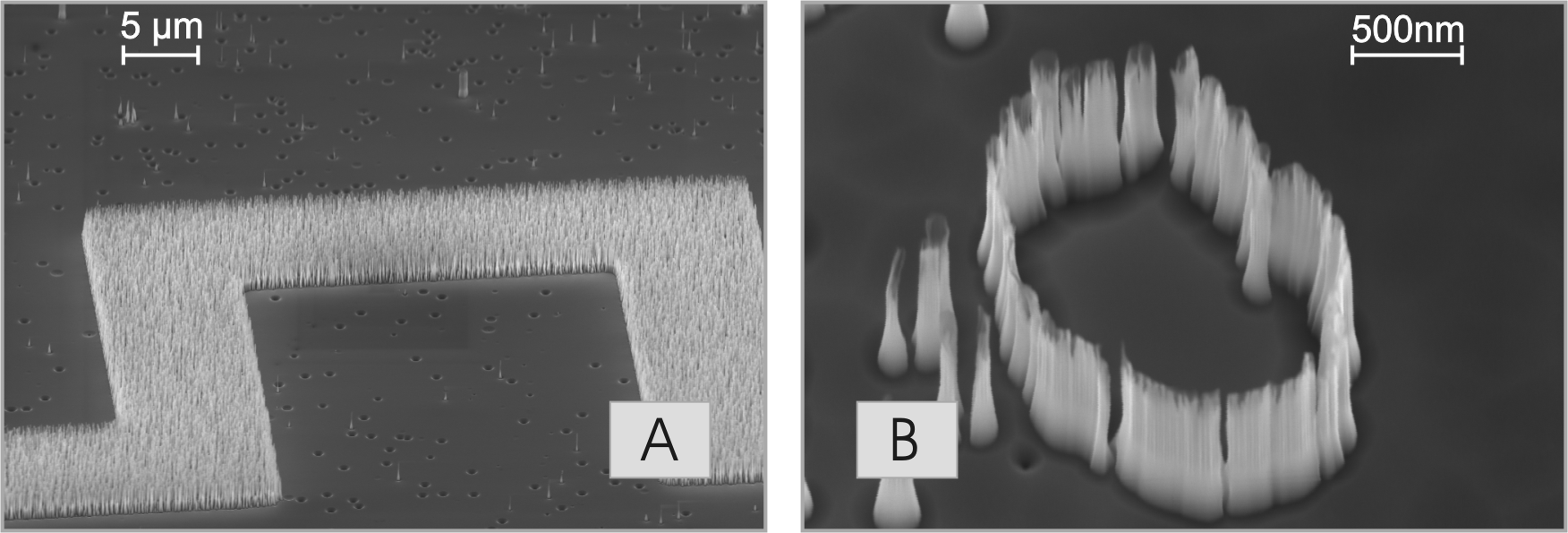
addition, we have observed a decreasing density of nanocolumns in
the areas without Ti micro-masking of the same etched samples
(Figure 5.3A). In those areas, the
nanocolumns density decreases dramatically, which indicates a
masking effect of different origin, probably due to Ga droplets
not removed before the processing. We can therefore suggest that,
unlike photoelectro-chemical (PEC) nanocolumn etching
[VRJ+01], the Ti ECR-RIE nanocolumns process is not dominated
by the influence of dislocations. Even if we cannot explain
completely the influence of the process parameters on the
nanocolumn formation, we have observed a good reproducibility of
the columns. Concerning the stability of the etching in relation
to the process parameters, further detailed structural
investigations are planned.
), no correlation can be found. In
addition, we have observed a decreasing density of nanocolumns in
the areas without Ti micro-masking of the same etched samples
(Figure 5.3A). In those areas, the
nanocolumns density decreases dramatically, which indicates a
masking effect of different origin, probably due to Ga droplets
not removed before the processing. We can therefore suggest that,
unlike photoelectro-chemical (PEC) nanocolumn etching
[VRJ+01], the Ti ECR-RIE nanocolumns process is not dominated
by the influence of dislocations. Even if we cannot explain
completely the influence of the process parameters on the
nanocolumn formation, we have observed a good reproducibility of
the columns. Concerning the stability of the etching in relation
to the process parameters, further detailed structural
investigations are planned.
In connection to the spatial control of the nanocolumns, some attempts have been performed using thin patterns realized by means of electron beam lithography. Despite the successful result shown in Fig. 5.3B, two problems need to be solved in this approach.
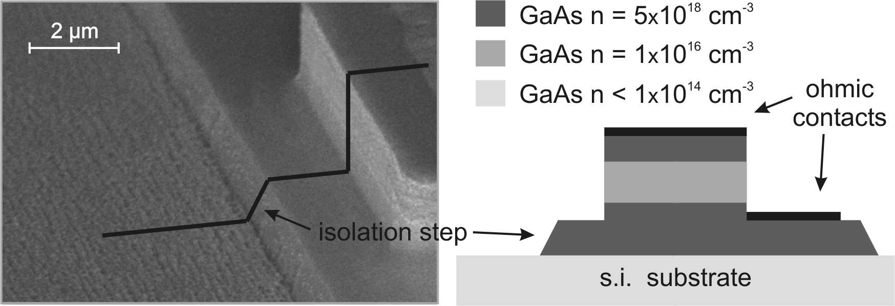
After the mesa etching, emitter (top) and collector (bottom) contacts are deposited. The electrical quality and the mechanical stability of the metal-semiconductor contacts play a determinant role concerning the efficiency and the lifetime of the Gunn diode. The special geometry and the vertical walls of the etched mesas allow a self-aligned approach, which means that both contacts are deposited at the same time and the division between emitter and collector is defined by the diode sidewall and not by a resist pattern. The self-aligned approach reduces the collector series resistance, minimizing the distance, which electrons have to drift in the bottom contact layer before entering in the metal conductor. Moreover, the process is simple and reliable, because it provides a high tolerance to lithography misalignment.
The considered contact technology produces an annealed ohmic contact (see also chapter 2.2.1). Thanks to the high doping at the interface metal-semiconductor, after the thermal treatment, the typical interface Schottky barrier becomes extremely thin. The barrier height is determined in both GaAs and GaN by the Fermi level pinning at the metal-semiconductor interface [Lüt95,IL03]. The thinner the barrier, the higher is the tunneling probability of the electrons crossing it.
The contact process flow is divided in three steps. At the beginning, the semiconductor surface has to be cleaned: the native oxide (about 1 nm) is removed from the surface by wet-chemical etching. Immediately after the cleaning, before the semiconductor oxidizes again, the metal is evaporated5.2. Then, the liftoff process is followed by the thermal annealing.
The chosen metal layer sequence for GaAs ohmic contacts is
Ge/Ni/Au. After the deposition, the sample is alloyed at 400
![]()
![]() C
for
C
for
![]() . For GaN Ti/Al/Ni/Au ohmic contacts have
been deposited and annealed at 900
. For GaN Ti/Al/Ni/Au ohmic contacts have
been deposited and annealed at 900
![]()
![]() C for
C for
![]() .
More details on the parameters of the two processes can be found
in appendix C.5 and in [Lep97,Jav03].
.
More details on the parameters of the two processes can be found
in appendix C.5 and in [Lep97,Jav03].
|
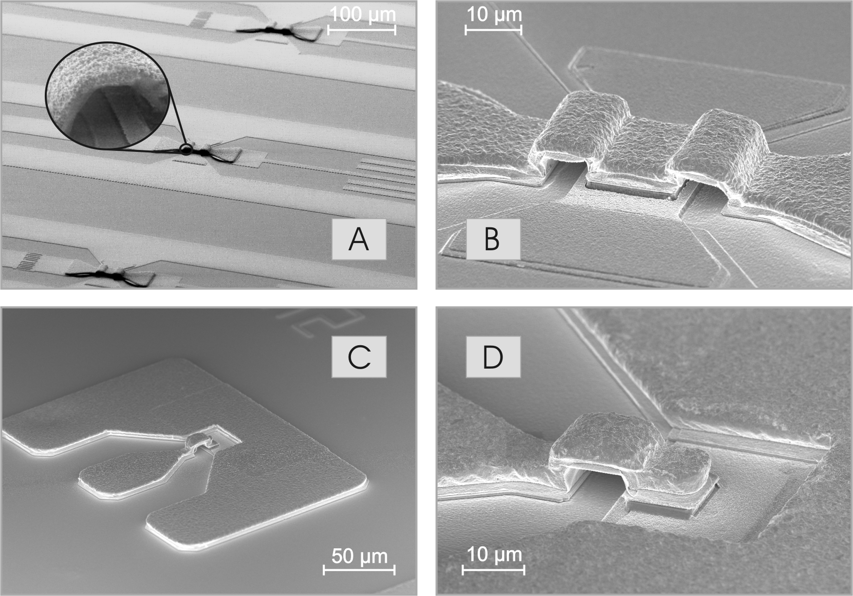
Figures 5.4A and B illustrate two ohmic contacts layouts, which are realized on GaAs, for the planar oscillator integration (two port configuration) and for the S-parameters measurements (one port configuration). The surface after the annealing is relatively flat and the contact edges are well-defined. It can be noticed that there is practically no separation between the mesa wall and the edge of the bottom metal contact (self-aligned lithography).
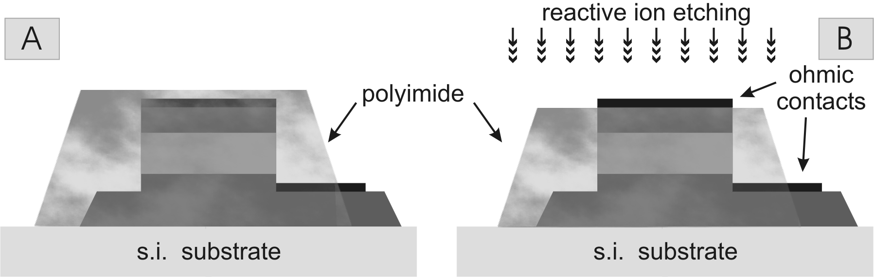
The GaAs diodes are covered with a positive thick resist pattern.
After the optical lithography, the sample is baked for about 20
minutes, in order to harden the resist and improve the adhesion.
Then, the open semiconductor material is removed down to the
semi-insulating substrate. About
![]() of GaAs is
etched with a sulfuric acid and oxygen peroxide solution. After
the wet-chemical etching, the hard resist mask can not be removed
simply with acetone and propanol, but it requires 30 minutes of
of GaAs is
etched with a sulfuric acid and oxygen peroxide solution. After
the wet-chemical etching, the hard resist mask can not be removed
simply with acetone and propanol, but it requires 30 minutes of
![]() plasma oven process. In Fig. 5.5, a GaAs
Gunn diode after the isolation treatment is presented. It is
interesting to notice the oblique slope provided by this etching;
the soft angle, in fact, acts as a ramp and it will be perfectly
covered by the metal pads, avoiding the connection breaks.
plasma oven process. In Fig. 5.5, a GaAs
Gunn diode after the isolation treatment is presented. It is
interesting to notice the oblique slope provided by this etching;
the soft angle, in fact, acts as a ramp and it will be perfectly
covered by the metal pads, avoiding the connection breaks.
|
Unfortunately, the GaAs process can not be directly transferred to
the GaN one. Due to the strong bond energies, which distinguishing
group III-nitrides from other compound semiconductors, it is
difficult to find suitable etching techniques. Wet chemical
etching is not applicable to GaN because of the low etch rates
and the problem to find an appropriate mask. The solution is
coming from argon ion sputtering. After protecting the GaN diodes
with thick resist, as described for GaAs, the sample is bombarded
by argon ions. The incident angle determines different etching
profiles. Too small incident angle leads to very steep sidewalls
and too high angle causes redeposition of etched material on
sidewalls. An angle of 30
![]()
![]() C represents a good compromise
[Jav03].
C represents a good compromise
[Jav03].
|
After the Duramide developing, the sample is baked in vacuum at
350
![]()
![]() C for one hour. During the hardening, Duramide undergo a
final polymerization and should not come in contact with oxygen.
The Duramide thickness is now measured with a profilometer:
typical values are between 5.6 and
C for one hour. During the hardening, Duramide undergo a
final polymerization and should not come in contact with oxygen.
The Duramide thickness is now measured with a profilometer:
typical values are between 5.6 and
![]() . Then,
the cured Duramide film is etched using a RIE process based on a
gas mixture of
. Then,
the cured Duramide film is etched using a RIE process based on a
gas mixture of ![]() and
and ![]() [Sto99]. Figure
5.6B, shows schematically the principle
behind the etching: the RIE process is stopped just after the
opening of the top contacts. Taking into account, that the
Duramide is not perfectly uniform on the sample (it is thicker at
the borders), an over-etch of
[Sto99]. Figure
5.6B, shows schematically the principle
behind the etching: the RIE process is stopped just after the
opening of the top contacts. Taking into account, that the
Duramide is not perfectly uniform on the sample (it is thicker at
the borders), an over-etch of
![]() is necessary.
is necessary.
|
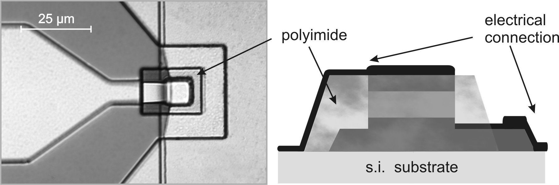
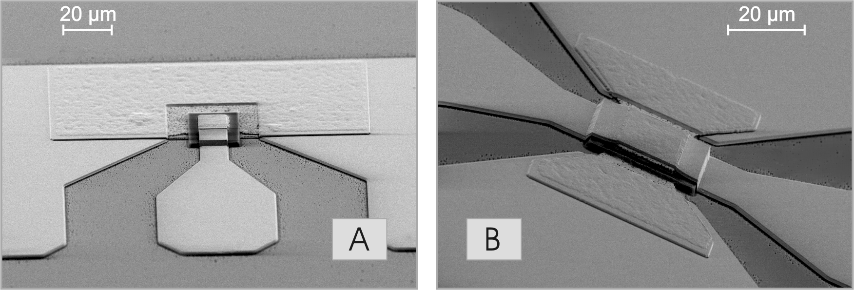
Figure 5.7, illustrates how the polyimide acts as a fundament for the connections. Unluckily, the polyimide is not a perfect ramp: some discontinuities could appear at the interface between the top contacts and the polyimide. For this reason, a special attention has been payed to the metal layers to be deposited. Also, the use of the rotating evaporation allows different incident angles for the incoming metal and a better coating of steep walls.
A special sequence of titan and gold (Ti/Au/Ti/Au,
50nm/50nm/50nm/650nm) has demonstrated excellent mechanical
properties regarding the discontinuity between the polyimide layer
and diode top contact. In Fig. 5.8, two SEM
pictures of the finished GaAs Gunn diodes are presented. In one
case, the diode is used for the S-parameters measurements (one
port configuration) and in the other one, it is part of the
integrated planar oscillator (two port configuration). The
dimensions of the CPW layouts are matched to
![]() lines.
lines.
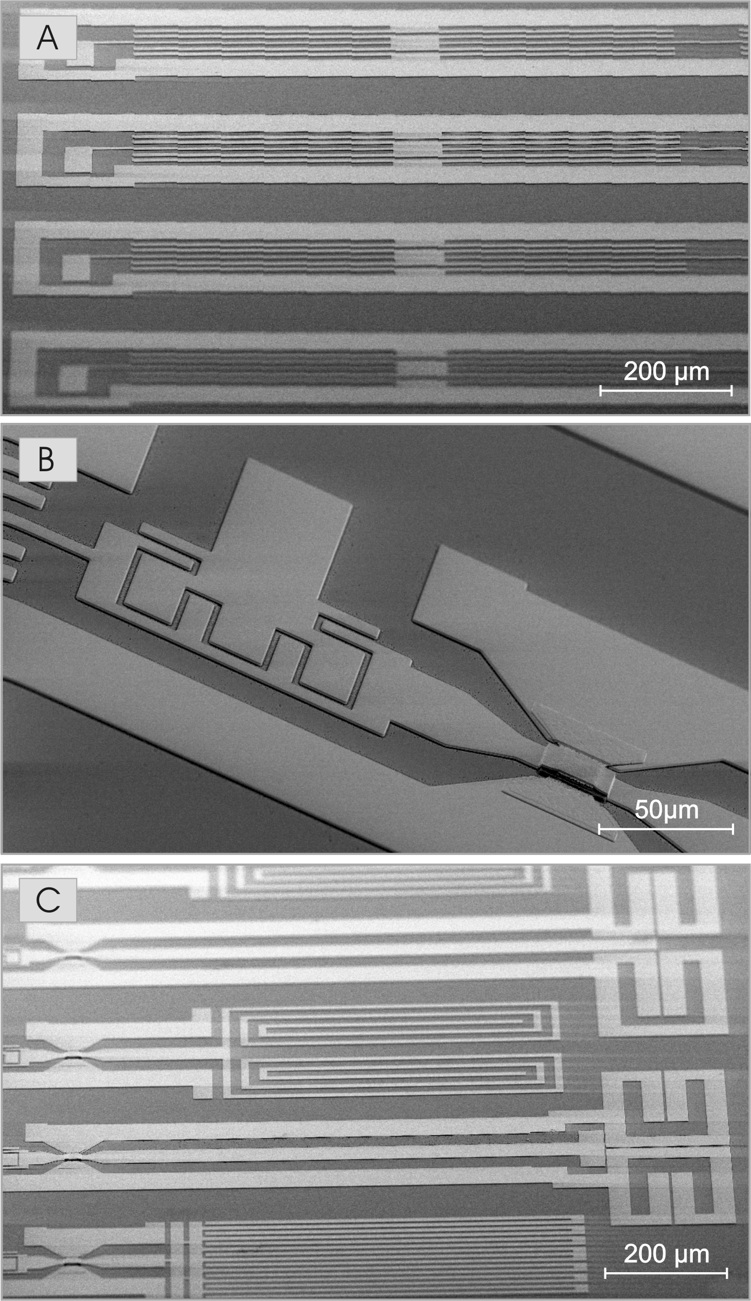
In Fig. 5.9, pictures of the GaAs MMIC Gunn diode oscillators are shown. The oscillators are composed of three parts: the periodic slow-wave low-pass filter (Fig. 5.9A), the interdigitated capacitor HF coupler (next to the Gunn diode Fig. 5.9B) and the different planar resonators (Fig. 5.9C).
|
|
For the air-bridge solution, the geometries and layout remain the same, except for the top contact connection, which is missing. Concerning the metal deposition, a simpler sequence (Ti/Au, 30nm/650nm) has been chosen. An alternative to the titanium layer could be chromium. Both metals exhibit a good adhesion to the substrate and once they are covered by gold, they do not oxidize. Ti/Au is a better option from the point of view of the lift-off process.
|
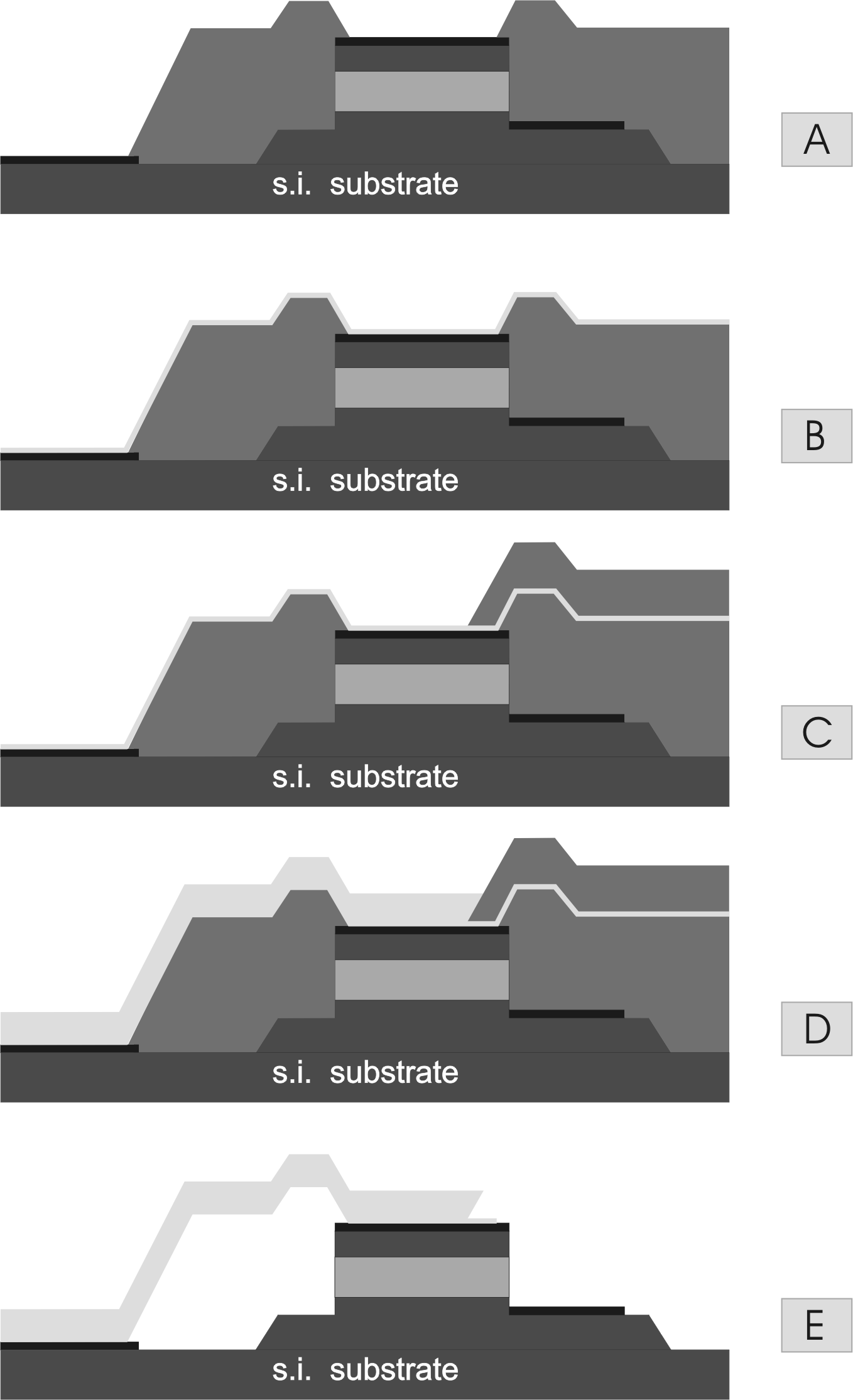
The fabrication of airbridges involves many steps (see Fig. 5.10). Two resist patterns are required to define the plated gold layer; the preplate and plate patterns work together to define the electroplated gold-metal level. Openings in the preplate resist are defined in the places that necessitate interconection (Fig. 5.10A). After the resist development, a prolonged bake has been performed (see appendix C.2). This postbake ensures a perfect dryness of the resist layer and prevents the process compromise during the next softbake step.
After the preplate pattern is processed, the sample is covered with a thin intermediate Cr/Au/Cr seed layer, which serves to carry the electroplating current (Fig. 5.10B). Alternatives are Au/Ti5.3 or only Au. Au/Ti prevents under-plating and Cr/Au/Cr provides a very good adhesion between the seed layer and the resist patterns. On the other hand, using only gold simplifies its removal later on. On top of the intermediate metal layer, a second resist is patterned to define the horizontal extent of any plated geometry, whether it is part of an air bridge or in contact with underlying metal (Fig. 5.10C).
For plating, a gold-bath from Enthone-Omi has been used. The
bath, which is based on a gold cyanide complex, is kept at a
temperature of 60
![]()
![]() C during plating. For more details on the
plating step, see appendix C.5.
C during plating. For more details on the
plating step, see appendix C.5.
After plating the intermediate metal, the two resist layers have
to be removed (Fig. 5.10E). The second
resist layer receives a long flood exposure and then is developed
away. 30 minutes of ![]() plasma etching cleans eventual remaining
traces. The intermediate seed metal from not plated areas is
etched with
plasma etching cleans eventual remaining
traces. The intermediate seed metal from not plated areas is
etched with
![]() solution or sputtered with argon ions.
Finally, the preplate resist is removed through boiling
acetone and 30min of
solution or sputtered with argon ions.
Finally, the preplate resist is removed through boiling
acetone and 30min of ![]() plasma etching.
plasma etching.
The fabricated gold airbridges, realized during the processing of the graded gap injector GaAs Gunn diodes, are shown in Fig. 5.11. Two typical layouts are presented: two port configuration for integrated planar oscillator (A and B) and one port configuration for S-parameter measurements (C and D).
simone montanari 2005-08-02