Decibelskalan
- This table shows voltage levels and corresponding dBV and dBu values. The text on the
page is in Swedish but the decibel table is useful without understanding Swedish.
How things work -
physical explanations how common things work
How to cheat with
dBs ... an intuitive approach - Decibels are relatively simple, yet many engineers
seem to have trouble doing the calculations mentally, here are few tips to make them
simpler
The
Printed Circuit Board Primer - A fine printed circuit board (PCB) is a mixture if high
art, and solid engineering. Here is a short primer on what goes into the making of a PCB,
the terminology, and the features that enhance reliabity, and lower cost.
Using a
multimeter - A meter is a measuring instrument. An ammeter measures current, a
voltmeter measures the potential difference (voltage) between two points, and an ohmmeter
measures resistance. A multimeter combines these functions, and possibly some additional
ones as well, into a single instrument.
Using the
Multimeter to Measure Voltage and Resistance - Multimeters are commonly used to
measure voltage and resistance between two points. Current is rarely measured because you
must alter the circuit to measure the current.
Alex's Giant
Glossary Listing - a large variety of Glossary and Acronym links pertaining to
electricity and electronics
Lexicon of
Semiconductor Terms - Intersil has assembled this Lexicon of Semiconductor Terms,
Abbreviations and Acronyms to improve understanding of the exciting world of
semiconductors.
The Hardware Tutor
- a complete beginner's guide to understanding how electronic circuits operate, written
from the perspective of a BASIC computer programmer
The Transistor
Story - The transistor was probably the most important invention of the 20th Century,
and the story behind the invention is one of clashing egos and top secret research.
Piezoelectricity education
- includes basic information, application data, FAQs, introduction to piezo transducers,
piezo history and recommended reading list
Spice runs
thermal analysis - performing a thermal analysis in Spice allows you to study a
circuit's electrical performance and the accompanying thermal effects simultaneously
Negatrons
enrich filter, oscillator designs - a test wave of high-performance op amps allows you
to incorporate "negatrons" (synthesized negative resistors) into your
oscillators and filters
Understanding Computers
- introduces signed and unsigned binary numbers, two's complements, the carry, borrow, and
overflow flags, and the effect of shifting signed and unsigned values, article is in pdf
format
EDA tools
let you track and control CMOS power dissipation - knowing where your chip is
dissipating power is important for both IC and chip-based system design and proper tools
and design techniques can help you analyze power consumption and make the right design
decisions
Field-programmable
devices - field-programmable devices come in a variety of fruity flavors, and more are
arriving all the time
S-88.110
DIGISKITTI - notes and information on a kit to help to learn basic digital circuit
operation by building your own circuits, text in Finnish
Some
designs send mixed signals - phrase "mixed signal" typically refers to
designs containing both analog and digital functions or components, but in the real world,
every electronic component behaves in an analog fashion, but you can connect these
components to form functions amenable to digital approximations
To be or not
to be asynchronous; that is the question - asynchronous logic conveys advantages in
certain situations, but, unlike synchronous logic, which you can typically view as a
series of sequential actions, you generally must view asynchronous logic concurrently
Both-ends
termination - Terminations exist to control ringing (sometimes called overshoot or
resonance). The best ways to control ringing on very long transmission lines are source
termination, end termination, and both-ends termination. The both-ends termination is
supremely tolerant of imperfections within the transmission system and within the
terminators themselves.
Breaking
up a pair - The two traces comprising a differential pair, when routed close together,
share a certain amount of cross-coupling, what happens when pair is breaking up
Crosstalk,
The Practical Way - Crosstalk introduced by neighboring nets, it’s noisiness
caused by signals from one net being coupled into other nets. Crosstalk can cause a
quiescent (static) clock or data line to cross a logic threshold when a neighboring net
switches and create timing violations, false clocking, and intermittent data faults. There
are several ways to prevent crosstalk on printed circuit boards.
Ground
Bounce in CMOS Devices - The high edge speeds and clock frequencies of advanced CMOS
technology can produce unwanted oscillations during logic level transitions resulting in
random logic bit errors.
Designing
for minimal jitter when using clock buffers - High-speed digital boards leave little
room for timing margin, certainly not enough to take jitter performance for granted.
Awareness of just a few key factors can yield superior performance by design.
Growing your
own IC clock tree - defining the clock-distribution network is one of the most
difficult aspects of high-speed digital systems and system-on-a-chip designs
Modeling
skin effect - Why does high-frequency current flow only on the outer surface of a wire
or a printed-circuit trace? Magnetic fields cause the behavior you describe. The technical
name for this property is the skin effect . It happens in all conductors.
Mysterious
ground - For single-ended measurements, don't depend on mysterious ground connections.
Always use a good, short ground connection.
Negative
Delay - The rule of causality prohibits the existence of a negative-delay circuit.
This article reveals how to make a negative-delay clock repeater, which is really just a
positive-delay circuit with a delay u set to a little less than one clock period. You can
easily implement a negative clock delay by using a coaxial cable of a suitable length.
PC-board
layout eases high-speed transmission - As digital techniques move to higher speeds,
designers become aware of the need to treat pc-board traces as RF transmission lines. In
these lines, you strive to hold the line impedance, Z0, to a constant value typically, and
to terminate the line with the same impedance. Data families such as ECL, PECL, and LVDS
send data over a pair of traces known as a balanced transmission line. If the traces are
on the top of a board with a ground plane under them, then you can model them as coupled
"microstrip" lines and if the traces are in a layer with ground planes above and
below them, then you can model them as coupled "striplines". This article gives
basic design information and dimensions tables for 50 ohm lines.
Practical
timing analysis for 100-MHz digital designs - As increasing chip complexity, high
clock rates, and analog signal-integrity issues complicate digital design, time-to-market
pressures continue to shorten development schedules. These factors present increasing
challenges to digital-design engineers. Most technical literature on high-speed design
focuses on termination, ringing, and crosstalk. Despite signal integrity's importance,
inadequate timing margins cause many more errors in today's 100-MHz digital designs.
Reducing
Emissions - Many hardware-design engineers use signal-integrity-analysis software to
check every trace on their boards for acceptable ringing, crosstalk, and delay. Often
during this process, the termination resistors are changed to ensure that the proper
voltage waveforms arrive at every receiver. Once the voltage waveforms are acceptable, the
design process is complete. This process is good enough for signal integrity, but it's not
good enough for EMI because most radiated-emissions problems depend more on signal
currents than on signal voltages.
Low-cost
circuit programs EEPROMs - When you migrate to 3.3V system supplies, you must usually
replace your old, reliable EEPROM programmer with a new, overly flexible and expensive
universal programmer. For less than $100, the circuit extends the functional life of any
5V EEPROM programmer. You can apply the circuit to any bidirectional 5 to 3.3V
level-translating application.
Tapered
transitions - Consider the problem of adapting a straddle-mount SMA connector for a
10-Gbps digital application. Exponential transitions are essential at high frequencies. A
1-in. exponential transition from the 0.060-in. SMA signal pad to a 0.010-in. trace should
provide startlingly good performance from dc to 10 GHz.
Two
transistors form bidirectional level translator - illustrates a translation from 5 to
3V, but it can accommodate almost any other voltage levels, provided the logic-low levels
are equal (usually 0V), translation from 1 to 100V are possible although slow
Two-transistor
circuit replaces IC - Linear Technology's recently introduced LTC4300 chip buffers I2C
clock and data lines to and from a hot-swappable card. This task is difficult because the
IC must work bidirectionally, meaning that you can simultaneously and actively drive both
sides. However, as is sometimes the case, you can replace a complicated circuit by a
simple one without much loss of performance. For example, transistors and resistors
replace the entire IC. Two npn transistors, connected head-to-head, form the heart of the
circuit. The two-transistor circuit offers the additional benefit of acting as a level
translator between two logic levels, for example 3.3V and 5V.
An analog-to-digital converter (also known as an ADC or an A/D
converter) is an electronic circuit that measures a real-world signal (such as
temperature, pressure, acceleration, and speed) and converts it to a digital
representation of the signal. A/D-converter compares the analog input voltage to a known
reference voltage and then produces a digital representation of this analog input. The
output of an ADC is a digital binary code. By its nature, an ADC introduces a quantization
error. This is simply the information that is lost, because for a continuous analog signal
there are an infinite number of voltages but only a finite number of ADC digital codes. By
increasing the resolution of the ADC, the number of discrete steps is increased, which
reduces quantization errors. Some A/D converters sample the input signal continuously,
whereas others sample at specific times. Any A/D converter that uses a track/hold buffer
must periodically connect its track/hold capacitor to the input signal, causing a small
inrush current.
A digital-to-analog converter (also known as a DAC or a D/A
converter) is an electronic circuit that converts a digital representation of a quantity
into a discrete analog value. The input to the DAC is typically a digital binary code, and
this code, along with a known reference voltage, results in a voltage or current at the
DAC output. The word "discrete" is very important to understand, because a DAC
cannot provide a continuous time output signal; rather, it provides analog
"steps." The steps can be lowpass-filtered to obtain a continuous signal.
All the sampling processes are limited by Nyquist limit. The Nyquist
limit is defined as half of the sampling frequency. The Nyquist limit sets the highest
frequency that the system can sample without frequency aliasing. In a sampled data system,
when the input signal of interest is sampled at a rate slower than the Nyquist limit (fIN
> 0.5fSAMPLE), the signal is effectively "folded back" into the Nyquist band,
thus appearing to be at a lower frequency than it actually is. This unwanted signal is
indistinguishable from other signals in the desired frequency band (fSAMPLE/2). Usually
the signals are prefiltered before they enter the A/D-converter to avoid too high
frequency signal components which can cause this kind of unwanted signals. In actual
practice, you should sample at a rate much higher than two times the Nyquist limit to
minimize sampling errors (general rule of thumb is 5 times higher that highest frequency
needed to be analyzed well). In some special applications frequency aliasing can also be
used in an advantageous manner (generally known as "undersampling" method).
In D/A conversion process the output of D/A converter is fed through
a filter which will remove the image-frequency information (signal higher than 1/2 of
sampling frequency) from the output signal. This image-frequency information can distort
the output signal. Two methods edist for removing unwanted image signals from the DAC
output to prevent alising in a following ADC. First approach is to use a high-performance
lowpass filter (data -> DAC -> high-order lowpass filter). For low pass filtering
usually a sixth-order lowpass filter is enough. The second methos is to use
digital-interpolation filters and a simple analogue filter (data -> oversampling
digital-interpolation filter -> DAC -> low-order lowpass filter).
16-bit
ADC provides 19-bit resolution - With aid of a programmable amplifier before A/D
conversion you can get more relative accuracy to the conversion.
ADC
grounding - Chip designers often internally partition the ground-reference net (or
substrate) for an ADC into isolated analog and digital regions for good reasons.
Improved
amplifier drives differential-input ADCs - ADCs with differential inputs are becoming
increasingly popular. This popularity isn't surprising, because differential inputs in the
ADC offer several advantages: good common-mode noise rejection, a doubling of the
available dynamic range without doubling the supply voltage, and cancellation of
even-order harmonics that accrue with a single-ended input. This document shows shows two
easy ways to create a differential-input differential-output instrumentation amplifier.
Multiple
ADC grounding - If you have a lot of ADCs on the same board and they all tie to the
same digital ground, then the various ADC grounds must all be somehow tied together. In a
low-resolution, 8-bit system, which needs only about 60 dB of noise rejection, you can use
one big, solid ground plane for all the analog channels and the digital logic. In higher
resolution systems requiring more noise isolation, you might worry about stray digital
currents flowing across the analog-ground region of your pc board.
The
beauty of differential drive - Even when sheer chaos is breaking out around an ADC,
differential-drive techniques can make the converter perform quietly
BountyQuest - site for
bounty hunters to sort out the good patents from the bad, rewards readers for finding
prior art information against listed patents
Dephion Intellectual Property
Network - lets you access over 26 years of U.S. Patent & Trademark Office (USPTO)
patent descriptions as well as the last 23 years of images, warlier known as IBM Patent
Server
Managing
intellectual property - ongoing series of articles explores why and how you should
take steps to protect your key technologies
Ownership
of Intellectual Property - In most circumstances, an engineer or software developer is
simply not entitled to ownership of the products that he develops on the job
Peter's Patent Page -
patent law page, listing of US patent firms and attorneys, patent information, patent
searching sites, IP organizations and articles
Electronic Symbol Libraries
- This site contains Electronic Component Symbol Libraries and Electronic Component
Mechanical Layout Libraries for AutoCad Version 12. Electronic Symbols are posted for free
individual use. The web page has also GIF pictures of the drawings in the libraries.
Schematic
Symbols - A diagram that shows passive components, resistors, capacitors and
inductors, and also electrical components such as switches, relays, motors and lamps. Also
diagram for active components.
MAGNETICS� Digital
Library. - This literature library can literature files can answer many questions and
assist with many magnetic core design challenges.
A
rudimentary resistor identifier - Select colors matching those of the resistor and get
the value of the resistor, needs a browser which supports JavaScript
ESD
Control for Electronics Manufacturing - this application note presents recommendations
for establishing basic ESD control equipment and practices in a small to mid-sized
manufacturing facility which handles sensitive electronics components and printed circuit
boards containing them
Building a
cost-effective soldering station - If there is one tool which is most important to the
DIY hi-fi hobbyist, it is the soldering iron. There are some jobs like soldering where you
won't produce a good job without a good tool. This document describes how you can build
your own solvering stating usind a Weller 'Magnastat' 24 volt iron with interchangeable
tips.
SMT
Desoldering Station - Working with SMT is quite difficult without an smt hot air
pencil . The prices of smt stations are too high , so you might consider to build it by
your own.
Soldering
technique reduces pc-board damage - in testing and troubleshooting surface-mounted
components, changing parts can be time consuming and easily damage the circuit board
Construction
Ideas - This document gives some ideas for constructing one-of-a-kind creations, where
designing and making PCBs often doesn't make sense.
Construction
Ideas - For most one-of-a-kind creations, designing and making PCBs often doesn't make
sense. This document gives you ideas how to use perf board, laminate board, ground plane
substrate, wood substrate and small plastic boxes.
Dead
Bug Prototyping for Effects - Some of you are familiar with "dead bug"
prototyping - named for the resemblance of a DIP IC flat on its back with its legs in the
air to a dead beetle. Dead bug style prototyping is usually only taken for a way to patch
in an IC with the wrong pinout, but it can be extended to other parts as well.
L�mp�mittarin
kotelo - Information how to make nice front panel to a box. This plans uses the front
panel graphics printed to a paper which is then laminated to the case. The text in
this document is in Finnish.
UHF
Construction Precautions - If you are building a kit or circuit that operates at VHF
(over 30 MHz) or UHF (over 300 MHz) you should be made aware of proper wiring and
construction practices. This is largely experience combined with a good theoretical
understanding.
Many different types of electrical and electronic devices are both
electrically-insulated and protected from the outside environment (heat, moisture,
touching, etc.) by putting them to a case. Most cases are made of plastic or metal.
Electronics modules made for very demanding environments (like car
electronics) are protected by potting them inside polymeric resins such as acrylics,
silicone and urethane. This potting encapsulation is usually done using two-part reactive
resins which are mixed then used. Encapsulation involves submerging an assembly into resin
(usually epoxy) and allowing the resin to harden. Epoxy potting protects circuit very
well. The obvious disadvantage to having circuits potted in epoxy is that they cannot
easily be repaired, as the components are inaccessible through the hard potting material.
It also works effectively in maintaining the security of the board design.
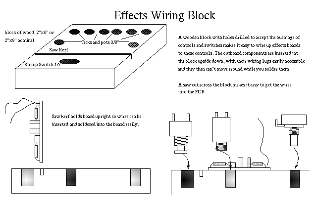
Effects
Wiring Block - A wooden block with holes drilled can be used to fasten the connectors
and controls plus the circuit board.
Encapsulation
/ Potting - Encapsulation provides effective dielectric resistance and environmental
protection while acting as an insulator against shock and vibration. It also works
effectively in maintaining the security of the board design.
Introduction
to ARP submodules Encapsulation Schemes - Early encapsulated circuit blocks typically
consisted of a small circuit board enclosed in a plastic case filled with epoxy potting
compound. Some modules filled with silicone rubber so that the circuit board and
components were covered, then sealed with a layer of epoxy, to make them somehow
repairable.
Really
Quick and Easy Boxes - Many plastic boxes are not strong enough for heavy touring use,
and being non-conductive, they will not shield against hum. To avoid humming all you
really need to do is to make the box conductive somehow. This document describes ho to do
that.
This section of web page describes how you can design and
manufacture your own printed circuit boards (PCBs). There are many techniques for making
PCBs, some of them are more suitable for low volume manufacturing and other are better for
high volume manufacturing in factories.
PCBs are great when mass-producing a device or when the circuit
complexity makes point-to-point wiring impractical.
Please note that making these PCBs involves some potentialy
hazardous chemicals and tools. It is your own resposibility to take suitable precautionary
actions! If you do not know what these suitable precautionary actions are, DO NOT use
these chemicals and tools. I recommend wearing protective goggles, clothing, and chemical
resistant gloves all the time when handling these chemicals, tools and PCBs!. In some
countries the use of some of the tools and chemicals may be bound to restrictions, such as
proper waste disposal and licenses, or may even be forbidden. For example both NaOH
(caustic soda) and Iron Cloride are very unhealthy if used carelessly.
General
EverythingPCB - web site
on PCB making information links
The
Printed Circuit Board Primer - A fine printed circuit board (PCB) is a mixture if high
art, and solid engineering. Here is a short primer on what goes into the making of a PCB,
the terminology, and the features that enhance reliabity, and lower cost.
Designing info
Crosstalk,
The Practical Way - Crosstalk introduced by neighboring nets, it’s noisiness
caused by signals from one net being coupled into other nets. Crosstalk can cause a
quiescent (static) clock or data line to cross a logic threshold when a neighboring net
switches and create timing violations, false clocking, and intermittent data faults. There
are several ways to prevent crosstalk on printed circuit boards.
PC-board
layout eases high-speed transmission - As digital techniques move to higher speeds,
designers become aware of the need to treat pc-board traces as RF transmission lines. In
these lines, you strive to hold the line impedance, Z0, to a constant value typically, and
to terminate the line with the same impedance. Data families such as ECL, PECL, and LVDS
send data over a pair of traces known as a balanced transmission line. If the traces are
on the top of a board with a ground plane under them, then you can model them as coupled
"microstrip" lines and if the traces are in a layer with ground planes above and
below them, then you can model them as coupled "striplines". This article gives
basic design information and dimensions tables for 50 ohm lines.
PCB maximum trace
current - The graph in this page shows the maximum printed circuit board (PCB) current
for given trace widths. The graph shows information for both 1-ounce and 2-ounce copper
traces. Outside layers of PCBs are generally available in 1-ounce and 2-ounce copper, a
reference to the weight of the copper per square foot of board. Inner layers of multilayer
boards can have 1/2-ounce copper. One-ounce copper is nominally 1.3435 mils or 0.0013435
inch thick. Good design practice limits temperature rise on FR4 board to 20�C
(MIL-STD-275C).
PCB Trace Impedance
Calculator - Calculates the characteristic impedance and per-unit-length parameters of
typical printed circuit board trace geometries. The source for formulas used in this
calculator (except where otherwise noted) is: IPC-D-317A, Design Guidelines for Electronic
Packaging Utilizing High-Speed Techniques, Jan 1995; Section 5, pp. 13 - 36.
PCB Trace Width
Calculator - This web calculator calculates the trace width for printed circuit boards
based on a curve fit to IPC-D-275.
How to make really
really good homemade PCBs - with the methods described, you can produce repeatably
good single and double-sided PCBs for through-hole and surface mount designs with track
densities of 40-50 tracks per inch and 0.5mm SM pitches
10 Steps
to Better Packaging Comm Infrastructure Designs - Given the rapidly evolving world of
communication equipment designs, it's often easy to forget about the nuts and bolts of
system packaging. What are the primary issues that need to be considered when packaging
electronics for a communication system? Whether it is an IP router, telco switch, or
wireless base station many of the design issues are the same.
Avoid
The Common Pitfalls When Designing Boundary-Scan Boards - IEEE 1149.1, or
"JTAG," has become one of the mainstream design-for-testability (DFT) techniques
and used to provide test coverage for circuit nets that aren't accessible by conventional
test probing
Designing
for reliability: a checklist - building products that stand the test of time requires
understanding reliability engineering and mathematics and must also understand reliability
prediction and a failure's effect on the user
EMI
and circuit components: where the rubber meets the road - You need to know how
components behave in the real world and what their limitations mean in terms of EMI. Some
guidelines in proper component selection for EMI and in designing simple EMI filters will
help in the battle.
Environmental-stress
screening improves electronic-design reliability - Environmental-stress screening is a
powerful tool for electronic-systems designers. Environmental-stress screening (ESS) is an
essential step in the design cycle of electronic systems, particularly as these systems
shrink in size and increase in complexity to satisfy the growing customer need for
low-power, portable, high-quality gadgets. ESS helps you design and develop highly
reliable products that will operate in different environments.
Hot-swapping
signals - Hot-swap designs were Once reserved for medical-support systems, telcomm, or
other "high-reliability" installations. now everybody wants to swap with the
lights on.
How To Draw
Schematic Diagrams - A well-drawn schematic makes it easy to understand how a circuit
works and aids in troubleshooting; a poor schematic only creates confusion. By keeping a
few rules and suggestions in mind, you can draw a good schematic in no more time than it
takes to draw a poor one. In this appendix we dispense advice of three varieties: general
principles, rules, and hints.
Keeping
embedded system design projects on time and close to budget - An all-too-common
mistake in the development of embedded control systems is to rush into the design process
with little or no appreciation for the full magnitude of the job, only to find oneself
with insufficient time or resources to do the job right.
Knowledge
of clocking aids ASIC-emulator choice - Real ASICs and software simulations differ
significantly. Though costly, ASIC emulators often help to bridge the gap. Recognizing the
trade-offs among emulator-design approaches can point you toward a wise investment.
Live
Insertion - Many applications require the ability to exchange modules in electronic
systems without removing the supply voltage from the module (live insertion). To avoid
damaging components, additional circuitry modifications are necessary. This document
describes in detail the phenomena that occur during live insertion and presents circuit
solutions for potential problems.
Lowpass
filter uses only two values - A low number of component values is advantageous for
low-cost manufacturing. This composite low-pass filter design uses four inductors of two
different values and five capacitors of two different values.
Predicting
Semiconductor Failure Modes - Electrostatic Discharge (ESD) is an invisible
destructive force that causes failure of electronic devices and reduces the reliability of
electronic systems
Product Usability
- How can designers make products that users will find usable?
Programmable
analogue ICs challenge Spice-and-breadboard designs - After years of
Spice-and-breadboard designing, analogue designers can now take advantage of increasingly
sophisticated programmable components and software-configuration tools. But how easy are
such components to use, and can they challenge traditional design approaches?
Sense
of self: enabling systems to monitor—and control—their environment - There's
nothing quite like having to explain to your boss that your entire network is down because
a $12 fan died. Proper management of the enclosure environment lets you pre-empt such
disastrous and embarrassing failures. The telecomm industry already demands high
availability, and if data communications wants to compete for voice and video services, it
needs to aim for a similar standard. To achieve efficient high availability, however, you
need to monitor a system to identify potential failures before they happen and actively
prevent them. Good system monitoring occurs on many levels.
Simple
design enhancements enable in-system test: part one - Many standard yet proprietary
strategies facilitate in-system test. Certain design features and enhancements minimally
affect product cost yet significantly expedite validating, manufacturing, and debugging of
silicon, thus reducing time to market and field failures.
Simple
design enhancements enable in-system test: part two - Many standard yet proprietary
strategies facilitate in-system test. Advanced design features and enhancements can
minimally affect product cost yet expedite validating, manufacturing, and debugging of
silicon, thus reducing time to market and field-failure cost.
Some Like
It Cool... - Remote comm equipment now resides in harsh environments, creating heat
dissipation problems. Designers must rethink thermal management to beat the elements.
Useful
Design-for-Test Practices - Successful DFT for deep-submicron system-on-a-chip ASIC
designs requires attention to detail from specification all the way through tape-out
