| pin # on the 100 pin Zorro slot | ZORRO 2 signal | pin # on the 86 pin expansion port | A500 signal and notes |
|---|---|---|---|
| 1 | GND | 1 | GND |
| 2 | GND | 2 | GND |
| 3 | GND | 3 | GND |
| 4 | GND | 4 | GND |
| 5 | +5 V | 5 | +5 V |
| 6 | +5 V | 6 | +5 V |
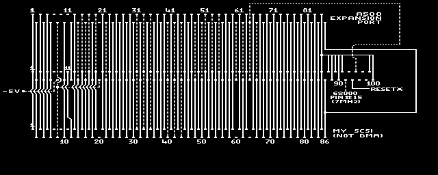
| 7 | LOCAL_OWN* | ??? | (not used by the Picasso II). This is an output signal to the Buster chip probably used for DMA. |
| 8 | -5 V | Some power supply | (not used by the Picasso II). This voltage is not present in the A500 power supply !!! In another hack (2000slot.lha) the author used the pin #8 of the expansion port but this gives -12 V !!!!! Watch out !!!! |
| 9 | SLAVEn* | ??? | (used by the Picasso II, but I leave it not connected). This is an output signal to the Buster chip probably used for DMA. |
| 10 | +12 V | 10 | +12 V |
| 11 | CONFIG_OUT* | - | this signal must go as CONFIG_IN* of the next board (I connected this to pin 12 of my SCSI controller inserted in the expansion port). See pic. |
| 12 | CONFIG_IN* | 12 | CONFIG*. NOTE: this signal must go only to one board (the Picasso) so you must break the connection between the #12 pin of the expansion port and the #12 pin of the board inserted into it. See pic. |
| 13 | GND | 13 | GND |
| 14 | C3* | 14 | C3* (not used by the Picasso II) |
| 15 | CDACB | 15 | CDAC (not used by the Picasso II) |
| 16 | C1* | 16 | C1* (not used by the Picasso II) |
| 17 | OVR* | 17 | OVR* (not used by the Picasso II) |
| 18 | XRDY | 18 | XRDY |
| 19 | INT2* | 19 | INT2* (not used by the Picasso II) |
| 20 | -12 V | 8 | -12 V (not used by the Picasso II) |
| 21 | BA5 | 21 | A5 |
| 22 | INT6* | 22 | INT6* (not used by the Picasso II) |
| 23 | BA6 | 23 | A6 |
| 24 | BA4 | 24 | A4 |
| 25 | GND | 25 | GND |
| 26 | BA3 | 26 | A3 |
| 27 | BA2 | 27 | A2 |
| 28 | BA7 | 28 | A7 |
| 29 | BA1 | 29 | A1 |
| 30 | BA8 | 30 | A8 |
| 31 | BFC0 | 31 | FC0 (not used by the Picasso II) |
| 32 | BA9 | 32 | A9 |
| 33 | BFC1 | 33 | FC1 (not used by the Picasso II) |
| 34 | BA10 | 34 | A10 |
| 35 | BFC2 | 35 | FC2 (not used by the Picasso II) |
| 36 | BA11 | 36 | A11 |
| 37 | GND | 37 | GND |
| 38 | BA12 | 38 | A12 |
| 39 | BA13 | 39 | A13 |
| 40 | EINT7* | 40 | IPL0* (not used by the Picasso II) |
| 41 | BA14 | 41 | A14 |
| 42 | EINT5* | 42 | IPL1* (not used by the Picasso II) |
| 43 | BA15 | 43 | A15 |
| 44 | EINT4* | 44 | IPL2* (not used by the Picasso II) |
| 45 | BA16 | 45 | A16 |
| 46 | BEER* | 46 | BEER* |
| 47 | BA17 | 47 | A17 |
| 48 | VPA* | 48 | VPA* (not used by the Picasso II) |
| 49 | GND | 49 | GND |
| 50 | E | 50 | E (not used by the Picasso II) |
| 51 | VMA* | 51 | VMA* (not used by the Picasso II) |
| 52 | BA18 | 52 | A18 |
| 53 | RST* | 53 | RST* (not used by the Picasso II) |
| 54 | BA19 | 54 | A19 |
| 55 | HLT* | 55 | HLT* (not used by the Picasso II) |
| 56 | BA20 | 56 | A20 |
| 57 | BA22 | 57 | A22 |
| 58 | BA21 | 58 | A21 |
| 59 | BA23 | 59 | A23 |
| 60 | BRn* | 60 | BR* (not used by the Picasso II). Used if the board uses DMA |
| 61 | GND | 61 | GND |
| 62 | BGACK* | 62 | BGACK* (not used by the Picasso II) |
| 63 | BD15 | 63 | D15 |
| 64 | BGn* | 64 | BG* (not used by the Picasso II). Used if the board uses DMA |
| 65 | BD14 | 65 | D14 |
| 66 | DTACK* | 66 | DTACK* (not used by the Picasso II) |
| 67 | BD13 | 67 | D13 |
| 68 | READ | 68 | R/w* |
| 69 | BD12 | 69 | D12 |
| 70 | BLDS* | 70 | LDS* |
| 71 | BD11 | 71 | D11 |
| 72 | BUDS* | 72 | UDS* |
| 73 | GND | 73 | GND |
| 74 | BAS* | 74 | AS* |
| 75 | BD0 | 75 | D0 |
| 76 | BD10 | 76 | D10 |
| 77 | BD1 | 77 | D1 |
| 78 | BD9 | 78 | D9 |
| 79 | BD2 | 79 | D2 |
| 80 | BD8 | 80 | D8 |
| 81 | BD3 | 81 | D3 |
| 82 | BD7 | 82 | D7 |
| 83 | BD4 | 83 | D4 |
| 84 | BD6 | 84 | D6 |
| 85 | GND | 85 | GND |
| 86 | BD5 | 86 | D5 |
| 87 | GND | 85 | GND |
| 88 | GND | 85 | GND |
| 89 | GND | 85 | GND |
| 90 | GND | 85 | GND |
| 91 | GND | 85 | GND |
| 92 | 7 MHz | 68000 pin #15 | (not used by the Picasso II) |
| 93 | DOE | ??? | (not used by the Picasso II). I think this signal is a delayed AS* (pin #74). The author of 2000slot used +5 V (pin #5 or #6). I think it is used by DMA boards |
| 94 | BUSRST* | - | I first tried the RST* signal (pin #53). It worked fine in 68000 mode, but I had big troubles in 68030 mode (yellow screen with flashing led). I solved all my problems using the A500 RESET* signal. I took this from the #11 pin of the U37 component of my rev.5 motherboard (it's a 74LS32 (NAND gates)). It is located under the internal floppy drive. If in your motherboard isn't there such component, you can try to follow the RST* signal track and see if it passes through some AND/NAND/OR... gate(s) and exits unchanged (AND with +5v, or OR with GND, ...) and then use the output as BUSRST*. |
| 95 | GBG* | 64 | BG* (not used by the Picasso II) |
| 96 | EINT1* | ??? | (not used by the Picasso II) |
| 97 | not connected | - | not connected |
| 98 | not connected | - | not connected |
| 99 | GND | 85 | GND |
| 100 | GND | 85 | GND |
Almost all the links are taken (shunt connection) directly from the 86 pin port, so you can solder a wire between the two corrisponding pins (one on the Amiga, the other on the new slot).
The CONFIG_IN* and CONFIG_OUT* signals are connected "serially": the CONFIG_IN*
from the 86 pin expansion port is connected to the Picasso's CONFIG_IN* pin;
the CONFIG_OUT* signal from the Picasso is connected to the CONFIG_IN* of the
board inserted in the 86 pin expansion port (e.g. my SCSI controller);
Probably it's possible to change the config order (first the SCSI controller,
then the Picasso) but my SCSI board has no CONFIG_OUT* signal.
NOTE: it's important that the CONFIG_IN* of the 86 pin expansion port goes to
only one board or you'll have auto-configuration conflicts !!
The BUSRST* signal is taken from a 74LS32 chip on the A500 motherboard (under the internal floppy drive); the 68000 RST* signal makes there a NAND (with negated inputs) with 0, thus it exits unchanged but more stable (and a little delayed), and then goes to the #94 pin of the Zorro 2 slot. I tried, before, to use directly the RST* signal as BUSRST* but I had some conflicts between the Picasso and the accelerating board during the reset sequence (I think both boards tried to autoconfig itself in the same time and/or in the same addresses).
I rate the realization quite simple if you are expert with soldering and
testing electric circuits, quite hard (and dangerous for your Amiga) if you
have no idea about what you're doing.
You had to be very patient and make everything slowly with calm.
It was impossible to me to found a 100 pin slot.
I went to a computer reparation center and there I obtained, for free, a
non-working 286 motherboard. I rip off from it 2 ISA (?) slots (62 pins
each); I cut it in the way that they can be aligned to form one 100 pin slot
(once the Picasso is inserted they won't move).
Then I used a 50 wires flat-cable (two 9 cm long pieces, aligned; keep these
cables as short as possible !) to make the connections between the 100 pin slot
and the 86 pin expansion port.
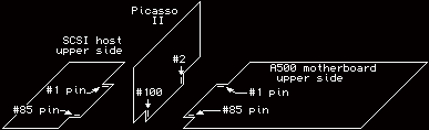
Note that the numer one pin on the A500 is to the rear of the upper side of
the motherboard, but the number one pin of the 100 pin slot is (looking at it
from above) to the rear of the left side.
I made all the solders in the "vias" (holes which bring a track from a face to the other) on the SCSI board; the SCSI board is inserted, with its slot, in the expansion port and the flat cables bring the signals to the new Zorro slot. Probably a look to some snapshots can explain it better.
If you can't do like me, probably you must think about some other way to
connect the boards; you can make a connector which duplicates the signal of the
expansion port (from each pin start two wires, one for the 100 pin slot and the
other for the SCSI controller).
Other wires can be used for the BUSRST*, 7MHz, -5V,... connections.
You have to make all the connections your new Zorro 2 board requires.
CHECK EVERYTIME IF THE CONNECTION ARE NOT FAULTY AND THERE ARE NO SHORT
CIRCUITS !!!
My brother Leonardo, for his insistence which push me to conceive and realize this project.
Dr. Segio Congiu, my Electronic Computers professor, who made me understand what I was doing.
My friends Massimiliano Farnea, Zeno Montresor, Michele Bianchi and Eugenio Perinelli for their technical,theorical and moral support.
Piergiorgio Sartor and Paolo Canali, ever ready and gentle to answer my technical questions.
The Amiga community of the Padova University, the worldwide Amiga community, the Amiga Report staff, the Amiga Internaional team, and everyone who knows me.